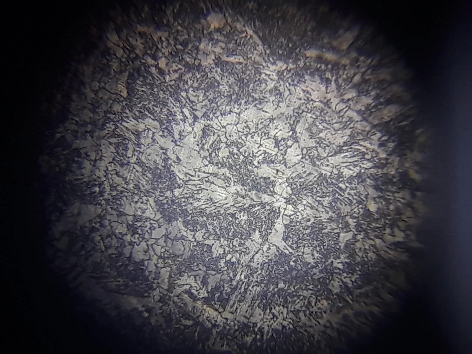
Analysing the grain structure of a TIG-welded billet.
In this article I am going walk you through how I managed to make this image (and more) of the crystallographic structure of a TIG-welded billet using my transmissive light microscope.
Conversion of the microscope
Since it is not possible to shine light through metallic objects/samples, a transmissive light microscope is not suitable for crystallographic analysis. An incident light microscope is needed instead. This type of microscope works by shining light onto the sample and this light being reflected back into the optics. This light needs to be fairly parallel to the optical axis of the lens system/optics of the microscope, or else very little light will be reflected directly into and through the lens system. Because of that, just shining a flashlight at the sample doesn’t work. I solved this problem by 3D-printing an adapter that clamps onto the left ocular and contains a white LED. I also added a diffusor made of a lightly sanded acrylic disc because the LED emits a pretty harsh, bright light. Now the light from the LED is coupled into the left ocular, shines onto the samples at a perfect 90° angle and gets reflected back into both oculars. Since the left ocular is blocked, only the right one can be used for observing the samples. However this is perfectly acceptable for making pictures.
I also added a potentiometer to be able to vary the intensity of the LED.
Preparing the sample
I made the sample by TIG-welding two pieces of mild steel (DC01/1.0330) together and sanding off the weld bead. I sanded up to 2000 grit (I would have preferred more, but this is what I had at home) in ~300 grit increments. Finally, I used some 1µm diamond lapping paste and a fine cloth to polish the surface to a mirror finish. This mirror finish is the most critical step of the preparation, without which you’d only see a scratchy mess under large magnifications.
After this, I etched the sample in Nital (3% nitric acid, 97% ethanol), which was generously supplied by my university. After etching the sample for about 20 seconds (depends on material), I quickly washed the Nital off with pure ethanol and then rinsed it with distilled water to prevent stains. This turned the mirror finish into a hazy white. This effect was more pronounced in the weld site as you can see below:
Looking at this sample with no magnification, you can already see different zones: The weld itself, the normalized grain and of course the base material (in that order, going up in the picture). You can also see a big pore in my weld but let’s ignore that for now. Generally, there are a lot more different zones in a weld, but I only made photos of those three, so we’ll only talk about them. At this point, the sample is ready for microscopy:
This is the normal base material at 400x magnification. You can see many different grain sizes, with some grains being quite big. This material does not seem to contain much perlite (dark stripey pattern indicating high carbon content), so I’d guess it contains relatively little carbon. This is confirmed by the datasheet: 0.12% C
This is the same material at the same magnifaction! The grain structure is a lot more uniform and contains much finer grains. This is the normalized zone, where the heat of the weld was high enough to normalize it, but not high enough to alter its structure in a more dramatic way.
This is the structure directly at the weld. This overheated structure contains spikey, almost dendrite-like structures, which indicate rapid heating and cooling, which is typical for welding. This structure is also called Widmannstätten-structure.
Now as you can see, it is absolutely possible to make really cool crystallographic images at home, if you have a microscope and the correct etchant! I’d highly recommend trying this out, since it is so much more exciting to see these structures in real life than just in textbooks.
As always, thanks for reading!


